
Hi everyone,
Time to catch up. As I am writing this, every single production part for the Solder Ninja Pen has been manufactured and is now being assembled. I am only days away from shipping, but before we get there, I want to look back at the manufacturing phase and finally share some behind the scenes footage I received from the suppliers over the summer. It is raw and unedited, but I think it provides an honest look at what making a product actually looks like. And I personally find it fascinating.
PCB Production and Assembly
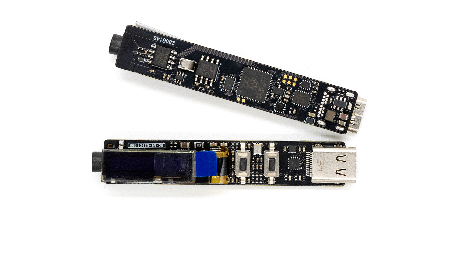
The circuit board is the functional core of the Solder Ninja Pen and it is not simple.
In a slightly questionable move, I began this project by fixing the outer diameter and length of the product before designing the electronics, which left me routing a PCB that was already smaller than what I was comfortable with at the time. When I later made the switch from an STM32 to an RP2040, I had to squeeze even more components and traces into the same form factor.
The result is a compact 59 by 11 mm, four-layer board, with components on both sides, often less than a millimeter away from the edge, most passives in 0402, a large number of vias, and even vias in pads. And the most absurd part? Because the design is cylindrical, the PCB has to be partially pocketed (also called z-axis milling) so that the 3.5 mm jack sits at the same height as the USB Type-C connector.
I remember painfully the hours spent on the first prototypes. I milled the PCBs in house, then soldered everything by hand under a binocular microscope, dreaming of the day when I could simply hand this off to someone with the right tools.

For production, I naturally turned to PCBWay. Yes, they sponsored part of the cost of this first batch, but my recommendation is genuine. After years in electronics I know what matters to me, and with their quick and efficient communication and their commitment to quality, I trust them with complex builds and atypical requests. They always deliver.
They shared some footage of the boards going through their assembly line. For those of you who might be unfamiliar with the process, it is quite impressive.
The boards are produced on panels that travel through the whole assembly sequence in one continuous automated flow. First, a stencil station deposits solder paste onto all required pads. The panel then enters a pick and place machine that positions every component at high speed with incredible precision. It then passes slowly through a controlled temperature profile in a reflow oven where the solder melts and bonds the components to the board. The same process happens on the second side. Followed by optical inspection to check solder joints and alignment.
Only one component cannot be assembled automatically. The OLED display uses a thin flexible cable that must be soldered by hand and PCBWay’s technicians handled this delicate step perfectly.
The boards I received were already depanelized and individually packed in ESD-safe bags. This avoids mechanical stress during separation and results in very clean edges. I was not expecting this level of care, and not all manufacturers take this extra step.
Traceability is something I take seriously, especially as a small hardware company. You can plan everything carefully, but over the lifespan of a product there will always be some amount of variability in parts and suppliers. If anything ever goes wrong, even years from now, it is important to quickly understand which units in the wild might be affected and which ones are not. That kind of clarity keeps any corrective action small and manageable.
For that reason, every Pen gets its own serial number and I keep track of the component lots that went into each unit. The serial number is written in EEPROM and flash, but I also wanted it to live on a part of the product that cannot fail electronically. The PCB is one element that is always present and always readable, so I was very happy to see that PCBWay offers per-board silkscreen numbering. It is a small detail, but it makes the whole traceability system much more robust.
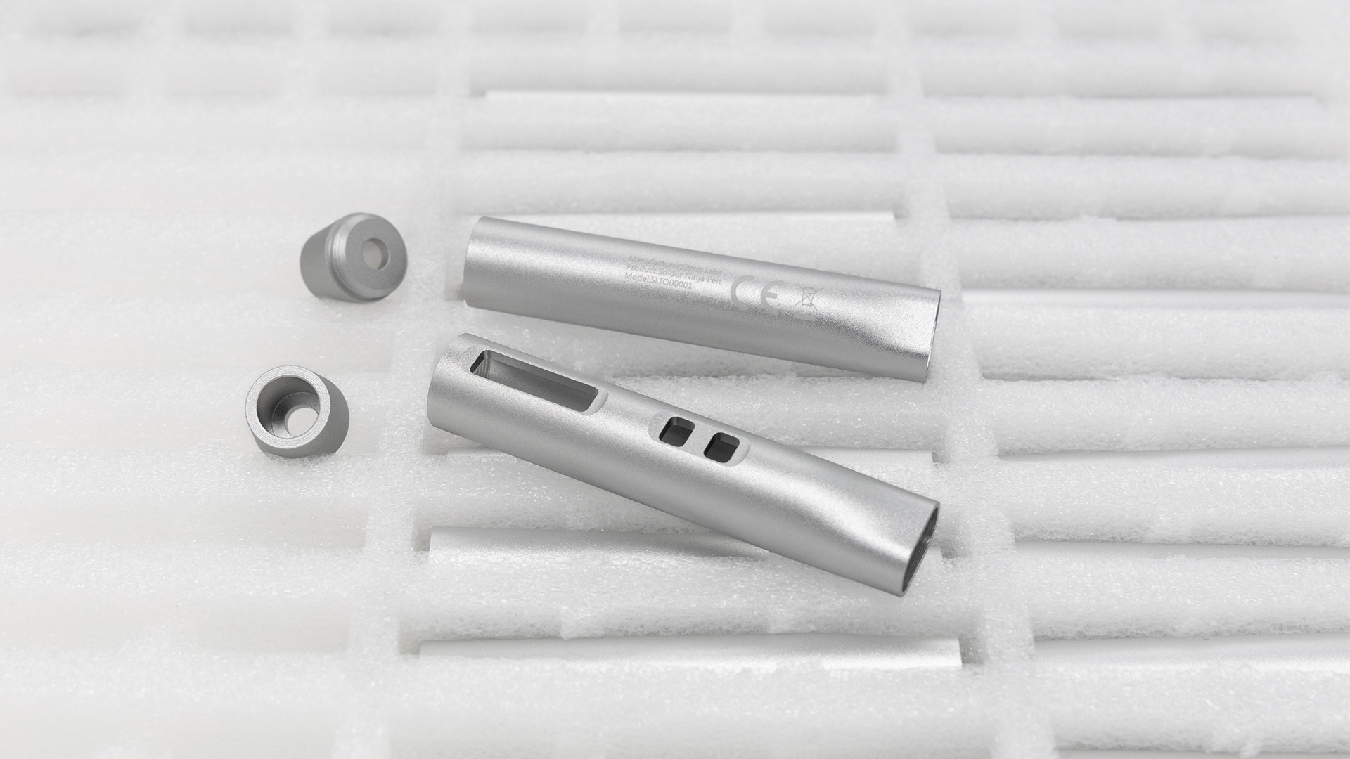
Aluminum Body Machining
The aluminum enclosure is the signature part of the Solder Ninja Pen, and also one of the trickiest to manufacture. The Pen consists of two threaded parts that screw into one another. There are no fasteners holding the PCB in place; instead, the body itself closes around it.
The larger part contains a very deep internal pocket. The difficulty of such a machining operation is often described by its depth-to-diameter ratio. A ratio of three is standard, and a ratio of five is already considered challenging. Here, we are close to ten, which requires specialized tooling and careful path planning. Then there is the fine thread connecting the two halves, with less than three millimeters of overlap, which also demands tight tolerances. The supplier had shown in earlier prototypes that they could achieve this reliably, but seeing the result at production scale was still impressive.
I designed the parts to be machined in two operations on a four-axis CNC machine, and that is exactly what you can see in the short video above.
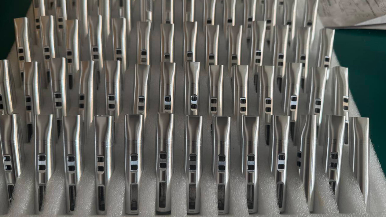
After machining, the parts are bead blasted, where fine abrasive particles are projected at high speed onto the aluminum to smooth out small machining marks and create an even texture. The parts are then anodized, which gives the Pen its final clean satin look and provides a hardened outer surface. Finally, each part is laser marked. This is not strictly required, since certification markings can legally appear only on the packaging or manual if they do not fit on the product, but I wanted the Pen itself to feel complete and professional. Marking a cylindrical part is not trivial because of laser focus, but the supplier handled it perfectly.
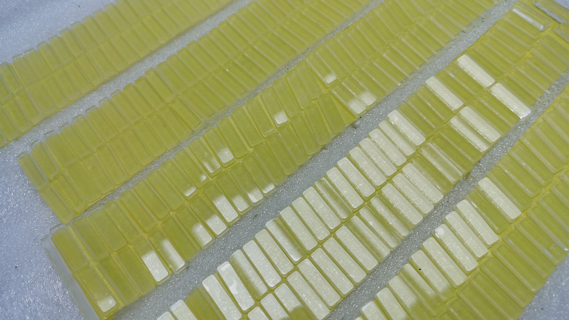
Acrylic Display Covers
The acrylic windows that protect the OLED are also CNC-machined so that they can fit into the curved profile of the body. There is nothing exotic about the process, but the manufacturer sent photos of the full production batch and there is something very satisfying about seeing hundreds of shiny, identical parts lined up.
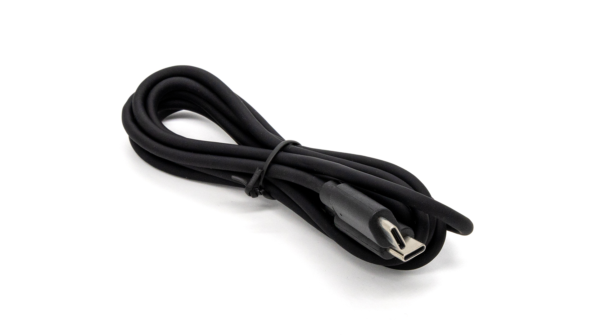
Final Cables
The cables also deserve a moment of attention. They look and feel great. Compared to the first batch, the silicone jacket went through an additional surface treatment, giving it an exceptionally smooth and soft touch finish. The connectors are slightly on the large side compared to the USB Type-C specification, so they may feel a bit tight the first time you plug them in, but that should disappear quickly. I have been using several of these production cables every day for weeks, bending them, coiling them, stuffing them in bags, and I am happy to report that they show no sign of fatigue. Good cables are easy to overlook, but they are a meaningful part of the experience of using a soldering iron like this.
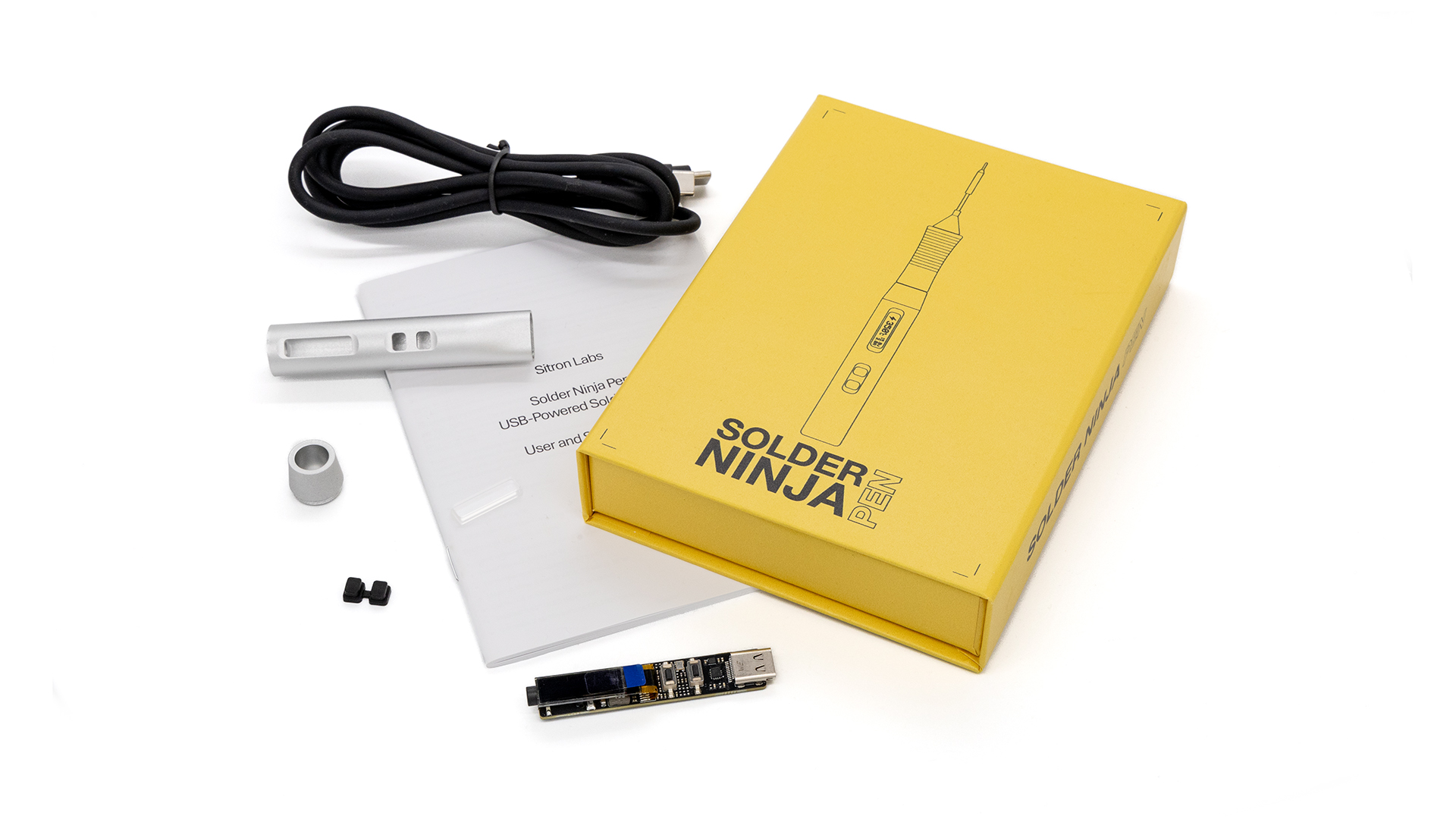
Everything on Hand
One of my favorite moments of the project was seeing all components finally come together. It is a strange mix of chaos and order, mostly chaos if I am honest, but it is also the point where everything suddenly feels very real.
What’s Next
The next update will focus on the in-house assembly and testing process. I built a dedicated test bench that programs and verifies every Pen. It is a small factory in itself, and I am looking forward to showing it.
Thank you again for your patience. We are very close.
Nicolas